Ddr sdram maximum volume. SDRAM memory: what do we have? What is SPD
– Organization and principles of work
– Physical organization
– Organization of SDRAM memory modules
– SPD chip
– Memory timings
– DDR/DDR2 SDRAM: Differences from SDR SDRAM
Organization and operating principles
Modern personal computers use standard memory SDRAM. This abbreviation stands for Synchronous Dynamic Random Access Memory - synchronous dynamic memory with random access.
Under synchronicity Usually we mean a strict binding of control signals and timing diagrams of memory operation to the system bus frequency. Generally speaking, the original meaning of the concept of synchronicity has already become quite conventional. Firstly, the memory bus frequency may differ from the system bus frequency (the existing “asynchronous” operating mode of DDR SDRAM memory, in which the processor system bus and memory bus frequencies can be correlated as 133/166 or 166/200 MHz). Secondly, there are systems in which the very concept of “system bus” becomes arbitrary - we are talking about AMD Athlon 64 class platforms with a memory controller integrated into the processor. The “system bus” frequency (which in this case does not mean the HyperTransport bus for exchanging data with peripherals, but the clock generator “bus” itself) in these platforms is only a reference frequency, which the processor multiplies by a given factor to obtain its own frequency. In this case, the memory controller always operates at the same frequency as the processor itself, and the memory bus frequency is set by an integer divisor, which may not coincide with the original “system bus” frequency multiplication factor. So, for example, the DDR-333 mode on the AMD Athlon 64 3200+ processor will correspond to a system bus frequency multiplier of 10 (processor and memory controller frequency 2000 MHz) and a memory frequency divider of 12 (memory bus frequency 166.7 MHz). Thus, "synchronous" SDRAM operation should currently be understood as strictly bound time intervals sending commands and data via the corresponding memory device interfaces to the memory bus frequency (in other words, all operations in RAM are performed strictly at the edge/fall of the memory interface clock signal). Thus, sending commands and reading/writing data can be carried out at each clock cycle of the memory bus (along the positive edge - the “edge” of the clock signal; in the case of DDR/DDR2 memory, data transfer occurs both along the “edge” and along the negative edge - the “cut” clock signal), but not at arbitrary time intervals (as was done in asynchronous DRAM).
The concept " dynamic"memory, DRAM, refers to all types of RAM, from the most ancient, “regular” asynchronous dynamic memory to modern DDR2. This term is introduced in contrast to the concept “ static"memory (SRAM) and means that the contents of each memory cell must be periodically updated (due to the peculiarities of its design, dictated by economic considerations). At the same time, static memory, characterized by a more complex and more expensive cell design and used as cache memory in processors (and previously on motherboards), is free from regeneration cycles, because it is based not on a capacitance (dynamic component), but on a trigger (static component).
Finally, it is also worth mentioning " random access memory» – Random Access Memory, RAM. Traditionally, this concept is opposed to devices " read-only memory» – Read-Only Memory, ROM. However, this opposition is not entirely correct, because from it we can conclude that ROM type memory is not random access memory. This is incorrect because ROM devices can be accessed in a random order rather than in a strictly sequential order. And in fact, the name "RAM" was originally used in opposition to early types of memory in which read/write operations could only be carried out in sequential order (for example, a tape drive). In this regard, the purpose and principle of operation of RAM is more correctly reflected by the abbreviation “RWM” (Read-Write Memory), which, however, is much less common. Note that the Russian abbreviations RAM and ROM - RAM (random access memory) and ROM (read-only memory), respectively, do not have such confusion.
The general principle of organization and operation of dynamic memory (DRAM) chips is practically the same for all its types - both the original asynchronous and modern synchronous. The exception is perhaps exotic options, which nevertheless existed even before the advent of SDRAM, such as Direct Rambus DRAM (DRDRAM). A DRAM memory array can be considered as a matrix (two-dimensional array) of elements, each of which contains one or more physical cells (depending on the configuration of the chip) capable of containing a basic unit of information - one bit of data. The cells are a combination of a transistor (switch) and a capacitor (memory element). Matrix elements are accessed using row address and column address decoders, which are controlled by RAS# (Row Access Strobe) and CAS# (Column Access Strobe) signals.
For reasons of minimizing the packaging size of the chip, row and column addresses are transmitted along the same address lines of the chip - in other words, they talk about multiplexing row and column addresses (the above-mentioned differences in the general principles of operation of DRDRAM chips from “regular” synchronous / asynchronous DRAM appear , in particular, here - the addresses of rows and columns are transmitted over different physical interfaces). So, for example, a 22-bit full cell address can be divided into two 11-bit addresses (row and column), which are sequentially (after a certain time interval determined by "timing" of memory) are fed to the address lines of the memory chip. Simultaneously with the second part of the address (column address), the corresponding command (reading or writing data) is sent via a single command-address interface of the SDRAM chip. Inside the memory chip, row and column addresses are temporarily stored in buffers ( latches) row addresses and column addresses, respectively.
It is important to note that a special buffer of static nature, called “ level amplifier"(SenseAmp), the size of which is equal to the size of one line, necessary for performing read operations and regenerating data contained in memory cells. Since the latter are physically capacitors that are discharged with each read operation, the level amplifier is required to restore the data stored in the cell after the access cycle is completed.
Additionally, since capacitors lose their charge over time (regardless of read operations), the cell contents must be refreshed periodically to prevent data loss. In modern types of memory that support automatic regeneration modes (in the “awakened” state) and self-regeneration(in a “sleeping” state), this is usually the task of the internal regeneration controller located directly on the memory chip.
In the most general case, the scheme for accessing a memory cell can be represented as follows:
1. The address of the line is supplied to the address lines of the memory chip. Along with this, the RAS# signal is issued, which places the address in the row address buffer (latch).
2. After the RAS# signal has stabilized, the row address decoder selects the desired row, and its contents are moved to the level amplifier (in this case, the logical state of the array row is inverted).
3. The address lines of the memory chip are supplied with the column address along with a CAS# signal, which places the address in the column address buffer (latch).
4. Since the CAS# signal also serves as a data output signal, as it stabilizes, the level amplifier sends the selected (corresponding to the column address) data to the output buffer.
5. The CAS# and RAS# signals are sequentially deactivated, allowing the access cycle to resume (after a period of time has passed during which the data from the level amplifier is returned back to the row cell array, restoring its previous logical state).
This is what the actual scheme for accessing a DRAM cell looked like in its very original version, implemented even before the appearance of the first actually used asynchronous memory chips/modules of the FPM (Fast Page Mode) DRAM type. However, it is easy to see that this scheme is quite suboptimal. Indeed, if we need to read the contents of not one, but several consecutive cells at once, differing only in the column address, but not in the row address, then there is no need to send the RAS# signal with the same row address each time (i.e., perform the steps 1-2). Instead, it is sufficient to keep the RAS# signal active for a period of time corresponding to, for example, four consecutive read cycles (steps 3-4, followed by deactivating CAS#), and then deactivating the RAS# signal. This is exactly the circuit used in asynchronous memory such as FPM DRAM and later EDO (Enhanced Data Output) DRAM. The latter was distinguished by advanced feeding of the address of the next column, which made it possible to achieve lower delays during read operations. In modern SDRAM chips, the scheme for accessing memory cells looks similar.
Physical organization
A DRAM chip is actually a two-dimensional array (matrix) of elements consisting of one or more elementary physical cells. Obviously, the main characteristic of this array is its capacity, expressed in the number of bits information that it can contain. You can often come across the concepts of “256-Mbit”, “512-Mbit” memory chips - we are talking about this parameter here. However, this capacity can be composed in different ways - here we do not mean the number of rows and columns, but the dimension or “capacity” of the individual element. The latter is directly related to the number of data lines, i.e. the width of the external data bus of the memory chip (but not necessarily with a proportionality coefficient of one, which will be seen below when considering the differences between DDR and DDR2 SDRAM memory and “regular” SDRAM). The data bus width of the very first memory chips was only 1 bit, but nowadays the most common are 4-, 8- and 16- (less often - 32-) bit memory chips. Thus, a 512 Mbit memory chip can be composed, for example, of 128M (134,217,728) 4-bit elements, 64M (67,108,864) 8-bit elements, or 32M (33,554,432) 16-bit elements - the corresponding configurations are recorded as "128Mx4", "64Mx8" and "32Mx16". The first of these numbers is called the depth of the memory chip (a dimensionless value), the second is the width (expressed in bits).
A significant distinguishing feature of SDRAM chips from earlier types of DRAM chips is that the data array is divided into several logical banks (at least 2, usually 4). This concept should not be confused with the concept of a “physical bank” (also called a “rank” of memory), defined for a module, but not a memory chip. The external data bus of each logical bank (as opposed to the physical one, which is made up of several memory chips to “fill” the memory controller data bus) is characterized by the same bit depth (width) as the bit width (width) of the external data bus of the memory chip as a whole (x4 , x8 or x16). In other words, the logical division of the microcircuit array into banks is carried out at the level of the number of elements in the array, but not the bit depth of the elements. Thus, the real examples of the logical organization of a 512-Mbit chip discussed above when it is “partitioned” into 4 banks can be written as 32Mx4x4 banks, 16Mx8x4 banks and 8Mx16x4 banks, respectively. However, much more often on the marking of memory chips one encounters configurations of “full” capacity, without taking into account its division into separate logical banks, while a detailed description of the organization of the chip (number of banks, rows and columns, width of the bank’s external data bus) can only be found in detailed technical documentation for this type of SDRAM chips.
The division of the SDRAM memory array into banks was introduced mainly for reasons of minimizing delays in the arrival of data into the system - after performing any operation with a memory line, after deactivating the RAS# signal, a certain time is required to “recharge” it. And the advantage of “multi-bank” SDRAM chips is that you can access a row of one bank while the row of another bank is “recharging”. You can arrange data in memory and organize access to it in such a way that further data will be requested from the second bank, already “recharged” and ready for use. At this moment it is quite natural to “recharge” the first bank and so on. This memory access scheme is called “bank interleave access”.
Organization of SDRAM memory modules
The main parameters of the logical organization of memory chips - capacity, depth and width - can be extended to physical memory modules such as SDRAM. The concept of capacity (or volume) of a module is obvious - this is the maximum amount of information that a given module can accommodate. Theoretically, it can be expressed in bits, but the “consumer” characteristic of a memory module is its volume (capacity), expressed in bytes - more precisely, given the current level of memory used - in mega- or gigabytes.
The width of the module is the width of its data bus interface, which corresponds to the width of the memory controller data bus and for all modern types of SDRAM memory controllers (SDR, DDR and DDR2) is 64 bits. Thus, all modern modules are characterized by the “x64” data bus interface width. The correspondence between the 64-bit width of the memory controller data bus (64-bit memory module interface) and the width of the external data bus of the memory chips, which is usually only 4, 8 or 16 bits, is achieved because the module data bus interface is composed of a simple serial " merging" external data buses of individual memory module chips. This “filling” of the memory controller data bus is usually called compiling a physical memory bank. Thus, to compose one physical bank of a 64-bit SDRAM memory module, it is necessary and sufficient to have 16 x4 chips, 8 x8 chips (this is the most common option) or 4 x16 chips.
The remaining parameter is the module depth, which is a characteristic of the capacity of the memory module, expressed in the number of “words” of a certain width, calculated by simply dividing the total volume of the module by the width of the external data bus (everything is expressed in bits). Thus, a typical 512MB SDR/DDR/DDR2 SDRAM memory module has a depth of 512MB * 8 (bits/bytes) / 64 bits = 64M. Accordingly, the product of the width by the depth gives the total capacity of the module and determines its organization, or geometry, which in this example is written as “64Mx64”.
When using sufficiently “wide” x8 or x16 chips, nothing prevents you from placing a larger number of them, corresponding to not one, but two physical banks - 16 x8 chips or 8 x16 chips. This is how they distinguish between single-bank (single-rank) and two-bank (dual-rank) modules. Two-bankMemory modules are most often represented by the “16 x8 chips” configuration, with one of the physical banks (the first 8 chips) located on the front side of the module, and the second of them (the remaining 8 chips) on the back. The presence of more than one physical bank in a memory module cannot be considered a definite advantage, because may require increased command interface delays, which are discussed in the corresponding section.
SPD chip
Even before the advent of the first type of synchronous dynamic random access memory (SDR SDRAM), the JEDEC standard stipulated that each memory module must contain a small specialized ROM chip, called a chip sequential presence detection(Serial Presence Detect, SPD). This chip contains basic information about the type and configuration of the module, time delays (“timings”) that must be adhered to when performing a particular operation at the memory chip level, as well as other information, including the module manufacturer code, its serial number, date manufacturing, etc. The latest revision of the SPD standard for DDR2 memory modules also includes data on the thermal operating conditions of the modules, which can be used, for example, to maintain optimal temperature conditions by controlling memory synchronization (the so-called " throttling memory", DRAM Throttle). More information about the SPD chip and what its contents look like can be found in the magazine article iXBT “SPD – sequential detection circuit”.
Timingsmemory
The theory behind the characteristics of memory chips/modules is “memory timings”. The concept of “timings” comes from delays that occur during any operations with the contents of memory cells due to the completely finite speed of operation of SDRAM devices as integrated circuits. Delays that occur during memory access are also commonly called memory “latency” (this term is not entirely correct and came into use with a literal translation of the term latency, meaning “delay”).
SDRAM chip data access scheme
1. Activating a row
Before performing any operation with data contained in a specific bank of the SDRAM chip (reading - READ command, or writing - WRITE command), it is necessary to “activate” the corresponding line in the corresponding bank. For this purpose, an activation command (ACTIVATE) is sent to the chip along with the bank number (lines BA0-BA1 for a 4-bank chip) and line address (address lines A0-A12, the actual number of which depends on the number of lines in the bank, in the example under consideration 512 -Mbit of SDRAM memory chip, their number is 213 = 8192).
The activated row remains open (available) for subsequent access operations until the command is received recharging the bank(PRECHARGE), essentially closing this line. The minimum period of “activity” of the line - from the moment of its activation until the moment the recharging command is received, is determined minimum line activity time(Row Active Time, tRAS).
Re-activation of any other row of the same bank cannot be carried out as long as the previous row of that bank remains open (i.e. the level amplifier containing a data buffer the size of one row of the bank and described in the section “SDRAM chips: Physical organization and principle of operation” is common to all lines of a given bank of the SDRAM chip). Thus, the minimum time interval between the activation of two different lines of the same bank is determined minimum line cycle time(Row Cycle Time, tRC).
At the same time, after activating a certain line of a certain bank, nothing prevents the SDRAM chip from activating any other line of another bank (this is the advantage of the “multi-bank” structure of SDRAM chips discussed above) on the next clock cycle of the memory bus. However, in real conditions, SDRAM device manufacturers usually also intentionally introduce an additional delay here, called delay between row activations(Row-to-Row Delay, tRRD). The reasons for introducing this delay are not related to the functioning of the memory chips as such and are purely electrical - the operation of activating a line consumes a very significant amount of electrical current, and therefore their frequent implementation can lead to unwanted excess current loads on the device.
2. Read/Write Data
The next time parameter for the functioning of memory devices arises due to the fact that the activation of a memory line itself requires a certain time. In this regard, subsequent (after ACTIVATE) commands for reading (READ) or writing (WRITE) data cannot be issued on the next clock cycle of the memory bus, but only after a certain time interval, delay between feeding row and column addresses(RAS#-to-CAS# Delay , tRCD ).
So, after a time interval equal to tRCD, when reading data, the READ command is sent to the memory chip along with the bank number (previously activated by the ACTIVATE command) and the column address. SDRAM memory devices are designed to read and write data in burst mode. This means that issuing just one READ (WRITE) command will lead to reading from cells (writing to cells) not one, but several consecutive elements, or “words” of data (the width of each of which is equal to the width of the external data bus of the microcircuit - for example, 8 bits). The number of data items read by one READ command or written by one WRITE command is called packet length(Burst Length) and usually amounts to 2, 4 or 8 elements (with the exception of the exotic case of transferring an entire line (page) - “Full-Page Burst", when it is necessary to additionally use the special BURST TERMINATE command to interrupt an extremely long packet data transfer). For DDR and DDR2 memory chips, the Burst Length parameter cannot take a value less than 2 and 4 elements, respectively, due to the features of their architecture.
There are two types of read command. The first of them is “regular” reading (READ), the second is called “reading with automatic recharging” (Read with Auto-Precharge, “RD+AP”). The latter differs in that after the completion of packet data transfer via the microcircuit data bus, the row recharging command (PRECHARGE) will be automatically issued, whereas in the first case, the selected row of the memory chip will remain “open” for further operations.
After issuing the READ command, the first portion of data is not immediately available, but with a delay of several clock cycles on the memory bus, during which the data read from the level amplifier is synchronized and transmitted to the external pins of the microcircuit. The delay between issuing a read command and the actual “appearance” of data on the bus is considered the most important and is probably known to many CAS# signal delay(CAS# Latency, tCL). Subsequent portions of data (in accordance with the length of the transmitted packet) are available without any additional delays at each subsequent clock cycle of the memory bus (1 element per clock for SDR devices, 2 elements in the case of DDR/DDR2 devices).
Data recording operations are carried out in a similar way. Similarly, there are two types of write commands - simple data writing (WRITE) and writing with subsequent automatic recharging of the line (Write with Auto-Precharge, “WR+AP”). Similarly, when the WRITE/WR+AP command is issued, the bank number and column address are sent to the memory chip. Finally, in the same way, data is written in a “batch” manner. The differences between a write operation and a read operation are as follows. Firstly, the first portion of data to be written must be sent via the data bus simultaneously with the WRITE/WR+AP command, bank number and column address being submitted via the address bus, and subsequent portions, the number of which is determined by the length of the packet, at each subsequent bus cycle memory. Secondly, instead of the “CAS# signal delay” (tCL), another characteristic called recovery period after recording(Write Recovery Time, tWR). This value determines the minimum amount of time between receiving the last piece of data to be written and the memory line being ready to be closed using the PRECHARGE command. If, instead of closing a row, a subsequent reading of data from the same open row is required, then another delay becomes important, delay between write and read operations(Write-to-Read Delay, tWTR).
3. Recharging the line
The cycle of reading/writing data into memory lines, which in general can be called a memory line access cycle, ends with closing the open line of the bank using the line recharging command - PRECHARGE, which can be issued automatically during the “RD+AP” or “WR+AP” operations " Subsequent access to this chip bank does not become possible immediately, but after an interval line recharging time(Row Precharge Time, tRP). During this period of time, the actual “recharging” operation is carried out, i.e. returning data elements corresponding to all columns of a given row from the level amplifier back to the cells of the memory row.
Relationships between timings
As stated above, to batch read a given amount of data (2, 4 or 8 elements), the following operations must be performed:
1. activate a line in a memory bank using the ACTIVATE command;
2. issue the READ data read command;
4. close the line using the PRECHARGE line recharging command (alternatively, this is done automatically if you use the “RD+AP” command in the second step).
The time interval between the first and second operation is the “delay between RAS# and CAS#” (tRCD), between the second and third - the “CAS# delay” (tCL). The time interval between the third and fourth operations depends on the length of the transmitted packet. Strictly speaking, in memory bus clock cycles it is equal to the length of the transmitted packet (2, 4 or 8), divided by the number of data elements transmitted over the external bus in one clock cycle - 1 for SDR devices, 2 for DDR devices. Let's call this value “tBL”.
SDRAM chips allow the third and fourth operations to be carried out almost "in parallel" in a sense. To be precise, the command to recharge the PRECHARGE line can be issued a certain number of clock cycles (x) before the moment at which the last data element of the requested packet is issued, without fear of a “break” situation in the transmitted packet (the latter will occur if the PRECHARGE command submit after the READ command with time period, less than x). Without going into details, it is enough to note that x is a value equal to the delay value of the CAS# signal minus one (x = tCL - 1).
The time interval between the fourth operation and the subsequent repetition of the first operation of the cycle is the “row recharge time” (tRP).
At the same time, the minimum time for a line to be active (from issuing the ACTIVATE command to issuing the PRECHARGE, tRAS command), according to his definition, is precisely the time interval between the start of the first and the beginning of the fourth operation. This leads to the first important relationship between memory timings:
min (tRAS) = tRCD + tCL + (tBL - (tCL - 1)) - 1.
The subtraction of one is due to the fact that the tRAS period does not include the clock cycle at which the PRECHARGE command is issued. Reducing this expression, we get:
min (tRAS) = tRCD + tBL .
The conclusion that follows from a detailed examination of the data access scheme contained in SDRAM memory is that the minimum value tRAS, oddly enough, does not depend on the delay value CAS#, tCL. The dependence of the former on the latter is a misconception that is quite often found in various manuals on RAM.
As an example first ratio Let's consider a typical high-speed DDR memory with delay values (tCL-tRCD-tRP) 2-2-2. With a minimum packet length of BL = 2 (the minimum possible for DDR), it is necessary to spend at least 1 memory bus clock cycle to transmit a data packet. Thus, in this case, the minimum tRAS value turns out to be 3 (such a small tRAS value does not allow setting the vast majority of memory controllers). Transmitting longer packets consisting of 4 elements (BL = 4, tBL = 2) increases this value to 4 clock cycles, finally, to transmit the maximum length of an 8-element packet (BL = 8, tBL = 4) the required minimum value of tRAS is 6 beats. It follows that since most memory controllers do not allow you to specify the tRAS value< 5, разумно настроить подсистему памяти таким образом, чтобы длина передаваемого пакета была максимальной (BL = 8, в том случае, если этот параметр присутствует в настройках подсистемы памяти в BIOS материнской платы), а величина tRAS принимала значение, равное 6. Альтернативный вариант – BL = 4, tRAS = 5.
Second important relationship between timings follows from the fact that the full cycle of batch data reading - from the 1st stage to its repetition - is called minimum line cycle time,tRC. Since the first three stages cannot take time less than tRAS, and the last takes time strictly equal to tRP, it follows:
tRC = tRAS + tRP.
Some memory controllers (for example, the integrated memory controller of AMD64 processors) allow you to independently set the tRAS and tRC timings, which, in principle, can lead to non-compliance with the above equality. However, there is some sense in this inequality will not have and only will mean that the value of one of the configured parameters (tRAS or tRC) will be automatically adjusted upward to maintain equality.
Scheme timings
The four most important parameters of memory timings, located in the following sequence: tCL-tRCD-tRP-tRAS, are usually called the “timing scheme”. Such schemes (for example, 2-2-2-5 or 2.5-3-3-7 for DDR memory; 3-3-3-9, 4-4-4-12 and 5-5-5-15 for memory type DDR2) can often be found in specifications for RAM modules.
Strictly speaking, this sequence does not correspond to the actual sequence of occurrence of delays when accessing the memory chip (for example, tRCD is located before tCL, and tRAS is “somewhere in the middle”), so in fact it reflects the main memory timings, arranged in order of their importance . Indeed, the most significant is the CAS# latency value (tCL), which manifests itself during each data read operation, while the tRCD and tRP parameters are relevant only for operations at the level of the memory line as a whole (its opening and closing, respectively).
Command interface delays
A special category of timings not related to access to data located in the cells of SDRAM chips can be considered command interface delays or their inverse characteristic - “command rate”. These delays are associated with the functioning of the memory subsystem at the level not of individual microcircuits, but of the physical banks they compose. When initializing the memory subsystem, each chip select signal associated with a specific physical memory bank is assigned a specific number in the chipset registers (usually according to the capacity of the physical banks - for example, descending), uniquely identifying this physical bank with each subsequent request (all physical banks share the same, common command/address and data buses). The more physical memory banks are present on a common memory bus, the greater the electrical capacitive load on it, on the one hand, and the greater the signal propagation delay (as a direct consequence of the length of the signal path) and the delay in encoding/decoding and the operation of the addressing and control logic, with another.
This creates delays at the command interface level, which are currently best known for platforms based on processors of the AMD Athlon 64 family with an integrated memory controller that supports DDR SDRAM memory. Of course, this does not mean that command interface delays are inherent only to this type of platform - for this type of platform, as a rule, in the memory subsystem settings in the BIOS there is a setting for the “Command Rate: 1T/2T” parameter, whereas in other modern platforms (for example , Intel Pentium 4 family with Intel 915, 925, 945, 955 and 975 series chipsets) there are no explicit command interface delay settings form and, apparently, are regulated automatically. On AMD Athlon 64 platforms, enabling the “2T” mode results in all commands being issued (along with the corresponding addresses) for not one, but two memory bus clock cycles, which seriously affects performance, but can be justified from the point of view in terms of the stability of the functioning of the memory subsystem.
DDR/DDR2 SDRAM: Differences from SDR SDRAM
Both types of chips (DDR SDRAM, SDR SDRAM), as a rule, have the same logical organization (with the same capacity), including a 4-bank organization of the memory array, and the same command-address interface. The fundamental differences between SDR and DDR lie in the organization of the logical data interface layer. Through the SDR SDRAM memory data interface, data is transmitted only along the positive edge (“edge”) of the clock signal. In this case, the internal operating frequency of SDRAM chips coincides with the frequency of the external data bus, and the width of the internal data bus of SDR SDRAM (from the cells directly to the I/O buffers) coincides with the width of the external data bus. At the same time, via the DDR memory data interface (as well as DDR2), data is transmitted twice in one clock cycle of the data bus - both along the positive edge of the clock signal (“edge”) and along the negative (“cut”).
The question arises: how can you organize double the data transfer rate in relation to the memory bus frequency? Two solutions are possible - you can either double the internal operating frequency of the memory chips (compared to the external bus frequency), or double the internal data bus width (compared to the external bus width). It would be quite naive to believe that the first solution was used in the implementation of the DDR standard, but it is quite easy to make a mistake in this direction, given the “purely marketing” approach to labeling DDR memory modules that supposedly operate at double the frequency (for example, DDR memory modules with real bus frequency of 200 MHz is called “DDR-400”). However, the second solution, which is used in devices such as DDR SDRAM, is much simpler and more effective - based on both technological and economic considerations. This architecture, used in DDR SDRAM, is called the “2n-prefetch” architecture. In this architecture, data is accessed “in pairs” - each single data read command results in sending two elements via the external data bus (the width of which, as in SDR SDRAM, is equal to the width of the external data bus). Similarly, each data write command waits for two elements to arrive on the external data bus. It is this circumstance that explains why the value of the “burst length” (Burst Length, BL) when transmitting data in DDR SDRAM devices cannot be less than 2.
DDR2 SDRAM devices are a logical continuation of the development of the “2n-prefetch” architecture used in DDR SDRAM devices. It is quite natural to expect that the architecture of DDR2 SDRAM devices is called “4n-prefetch” and implies that the width of the internal data bus is no longer two, but four times larger compared to the width of the external data bus. However, we are not talking here about a further increase in the number of data units transmitted per clock of the external data bus - otherwise such devices would no longer be called “Double Data Rate 2nd generation” devices. Instead, further “expansion” of the internal data bus allows the internal operating frequency of DDR2 SDRAM chips to be reduced by half compared to the operating frequency of DDR SDRAM chips with the same theoretical bandwidth. On the one hand, reducing the internal operating frequency of microcircuits, along with reducing the nominal supply voltage from 2.5 to 1.8 V (due to the use of a new 90-nm technological process), makes it possible to significantly reduce the power consumed by memory devices. On the other hand, the 4n-prefetch architecture of DDR2 chips allows you to achieve twice the frequency of the external data bus compared to the frequency of the external data bus of DDR chips - with the same internal operating frequency of the chips themselves. This is exactly what is currently observed - memory modules of the standard speed category DDR2-800 (data bus frequency 400 MHz) are quite common in the memory market today, while last official The DDR standard is limited to the speed category DDR-400 (data bus frequency 200 MHz).
What is SDRAM?
Synchronous random access memory (SDRAM) is the first random access memory (DRAM) technology designed to synchronize memory operation with CPU clock cycles on an external data bus. SDRAM is based on standard DRAM and works almost the same as standard DRAM, but it has several distinctive characteristics that make it more advanced:
Synchronous operation SDRAM, unlike standard and asynchronous DRAMs, has an input timer, so the system timer, which incrementally controls the microprocessor's activity, can also control SDRAM operation. This means that the memory controller knows the exact timer cycle on which the requested data will be processed. As a result, this frees the processor from having to wait between memory accesses.
General properties of SDRAM
- Synchronized by clock cycles with the CPU
- Based on standard DRAM, but significantly faster - up to 4 times
- Specific properties:
synchronous functioning,
alternating cell banks,
ability to work in batch-conveyor mode- Leading contender for use as main memory in next-generation personal computers
Cell banks are memory cells inside an SDRAM chip that are divided into two, independent cell banks. Since both banks can be active simultaneously, a continuous data flow can be achieved by simply switching between banks. This technique is called interleaving, and it reduces the overall number of memory access cycles and, as a result, increases data transfer speed. Burst acceleration is a fast data transfer technique that automatically generates a block of data (a series of sequential addresses) every time the processor requests one address. Based on the assumption that the next data address to be requested by the processor will be the next one relative to the previous requested address, which is usually true (this is the same prediction that is used in the cache algorithm). Batch mode can be used for both read operations (from memory) and write operations (to memory).
Now about the phrase that SDRAM is faster memory. Even though SDRAM is based on standard DRAM architecture, the combination of the above three characteristics allows for a faster and more efficient data transfer process. SDRAM can already transfer data at speeds up to 100MHz, which is almost four times faster than standard DRAM. This puts SDRAM on par with the more expensive SRAM (static RAM) used as external cache memory.
Why SDRAM?
Because the computer's RAM stores information that the CPU requires to function, the time it takes for data to pass between the CPU and memory is critical. A faster processor can only improve system performance if it doesn't get caught in a "hurry up and wait" loop while the rest of the system struggles to stay in that state. Unfortunately, since Intel introduced its x286 processor fifteen years ago, conventional memory chips have no longer been able to keep up with the enormously increased performance of processors.
Standard, asynchronous DRAM operates without timer input control, which was not required for data transfer until the second decade of microprocessor development. From this point on, systems with faster processors that use standard DRAM must force sleep states (time delays) to avoid memory overflow. A sleep state is when the microprocessor suspends execution of whatever it is doing until other components move on. into command receiving mode. For this reason, new memory technologies are being introduced not only to increase the exchange speed, but also to reduce the cycle of searching and retrieving data. In the face of these demands, memory chip manufacturers introduced a series of innovations including page mode memory, static column memory, interleaved memory, and FPM DRAM (fast page mode). As processor speeds increased to 100MHz and higher, system designers introduced small, high-speed external SRAM (Level 2 cache) caches for use, as well as new high-speed EDO (Extended Data Access) and BEDO (Batch Extensible Access) memories. FPM DRAM and EDO DRAM are the most commonly used memories in modern PCs, but their asynchronous circuitry is not designed for speeds greater than 66MHz (maximum for BEDO). Unfortunately, this factor limits today's systems, based on Pentium-type processors with clock speeds of more than 133MHz, to a memory bus frequency of 66MHz.
The emergence of SDRAM.
Initially, SDRAM was proposed as a lower-cost alternative to expensive VRAM (Video RAM) used in graphics subsystems. However, it quickly found use in many applications and became the number one candidate for the role of main memory for the next generations of PCs.
How does SDRAM work?
SDRAM is based on standard DRAM and works the same as standard DRAM - accessing rows and columns of data cells. Only SDRAM combines its specific properties of cell bank synchronous operation and burst operation to effectively eliminate latency-wait conditions. When the processor needs to get data from RAM, it can get it at the right time. Thus, the actual processing time of the data did not directly change, in contrast to the increase in the efficiency of data sampling and transmission. To understand how SDRAM speeds up the process of fetching and retrieving data in memory, imagine that the central processing unit has a messenger who pushes a cart around the RAM building, and each time he needs to drop or pick up information. In a RAM building, the clerk responsible for forwarding/receiving information typically spends about 60ns to process the request. The messenger only knows how long it takes to process the request after it is received. But he doesn't know whether the clerk will be ready when he arrives, so he usually allows a little time in case of a mistake. He waits until the clerk is ready to receive the request. It then waits for the usual time required to process the request. And then, he pauses to check that the requested data is loaded into his cart before taking the data cart back to the CPU. Suppose, on the other hand, that every 10 nanoseconds the sending clerk in the RAM building must be outside and ready to receive another request or to respond to a request that was previously received. This makes the process more efficient since the messenger can arrive at exactly the right time. Processing of the request begins the moment it is received. Information is sent to the CPU when it is ready.
What are the performance benefits?
Access time (commands to address to data fetch) is the same for all memory types, as can be seen from the table above, since their internal architecture is basically the same. A more telling parameter is cycle time, which measures how quickly two sequential accesses can be made on a chip. The first read cycle is the same for all four types of memory - 50ns, 60ns or 70ns. But the real differences can be seen by looking at how quickly the second, third, fourth, etc. are completed. reading cycle. To do this, we will look at the cycle time. For "-6" FPM DRAM (60ns), the second cycle can be completed in 35ns. Compare this to "-12" SDRAM (60ns access time), where the second read cycle takes 12ns. This is three times faster, and at the same time, without any significant reworking of the system!
The most significant performance improvements when using SDRAM are:
- Faster and more efficient - nearly four times faster than standard DRAM
- Potentially could replace the more expensive EDO/L2 cache combination that is now the standard
- "When running synchronously" - eliminates time constraints and does not slow down the latest processors
- Internal interleaving of dual bank operations promotes continuous data flow
- Possibility of batch operation up to a full page (using up to x16 chips)
- Pipeline addressing allows the second data requested to be accessed before the first data requested is completed.
What is the place of SDRAM among future PC memory?
Currently, FPM DRAM and EDO DRAM make up the majority of mainstream PC memory, but SDRAM is expected to quickly become the primary alternative to standard DRAM. Upgrading from FPM memory to EDO (plus L2 cache) increases performance by 50%, and upgrading from EDO to BEDO or SDRAM provides an additional 50% performance boost. Still, many suppliers of ready-made systems see BEDO only as an intermediate step between EDO and SDRAM due to the inherent speed limitations of BEDO. The SDRAM they expect will be the main memory when selected.
Current needs come from graphics-intensive and computationally intensive applications such as multimedia, servers, digital set-top boxes (systems for home use that combine a TV, stereo system, web browser, etc.), switches ATM, and other network and communications equipment requiring high throughput and data transfer rates. In the near future, however, industry experts predict that SDRAM will become the new memory standard in personal computers.
The next step in the development of SDRAM has already been made, this is DDR SDRAM or SDRAM II
And Samsung, known as the largest manufacturer of SEC-labeled memory chips, took this step. The release of the new memory will be officially announced in the near future, but some details are already known. The name of the new memory is "Double Data Rate SDRAM" or simply "SDRAM II". The catch is that the new synchronous memory can transfer data on the rising and falling levels of the bus signal, which allows increasing bandwidth to 1.6 GB/sec at a bus frequency of 100 MHz. This will double the memory bandwidth compared to existing SDRAM. It is stated that the new VIA VP3 chipset will provide the ability to use new memory in systems.
Be careful when choosing SDRAM for use in systems based on the i440LX chipset
Double Data Rate Synchronous Dynamic Random Access Memory - synchronous dynamic memory with random access and double data transfer rate) - a type of computer memory used in computing as RAM and video memory. It replaced SDRAM type memory.As practice has shown, motherboards made on the basis of the latest i440LX chipset are very sensitive to the type of SDRAM memory used. This is due to the fact that the new Intel SPD specification for SDRAM defines additional requirements for the content of special information about the DIMM module used, which must be located in a small element of electronically programmable memory EPROM located on the memory module itself. However, this does not mean that any SDRAM module with an EPROM on it complies with the SPD specification, but in particular, it means that a module without an EPROM does not exactly comply with this specification. Some boards based on the i440LX set require only such special modules to operate, but most of the existing ones work perfectly with regular SDRAM modules. This step by Intel to introduce a standard for synchronous memory modules is associated, first of all, with the desire to ensure reliable operation and compatibility of memory with the future i440BX chipset, which will already support a bus frequency of 100MHz.
When using DDR SDRAM, twice the operating speed is achieved than in SDRAM, due to reading commands and data not only on the edge, as in SDRAM, but also on the fall of the clock signal. This doubles the data transfer rate without increasing the memory bus clock frequency. Thus, when DDR operates at 100 MHz, we will get an effective frequency of 200 MHz (when compared with the SDR SDRAM analogue). The JEDEC specification makes a note that it is incorrect to use the term “MHz” in DDR; the correct rate is “millions of transfers per second per data pin.”
The specific operating mode of memory modules is dual-channel mode.
Description
DDR SDRAM memory chips are produced in TSOP packages and (later mastered) BGA (FBGA) packages, manufactured according to 0.13 and 0.09-micron process standards:
- IC supply voltage: 2.6 V +/- 0.1 V
- Power consumption: 527 mW
- I/O Interface: SSTL_2
The memory bus width is 64 bits, that is, 8 bytes are simultaneously transferred along the bus in one clock cycle. As a result, we obtain the following formula for calculating the maximum transfer rate for a given memory type: ( memory bus clock speed)x 2 (data transfer twice per clock) x 8 (number of bytes transmitted per clock cycle). For example, to ensure data transfer twice per clock cycle, a special “2n Prefetch” architecture is used. The internal data bus is twice as wide as the external one. When transmitting data, the first half of the data bus is transmitted first on the rising edge of the clock signal, and then the second half of the data bus on the falling edge.
In addition to double data transfer, DDR SDRAM has several other fundamental differences from simple SDRAM. Basically, they are technological. For example, a QDS signal has been added and is located on the PCB along with the data lines. It is used for synchronization during data transfer. If two memory modules are used, then the data from them arrives at the memory controller with a slight difference due to the different distance. A problem arises in choosing a clock signal for reading them, and the use of QDS successfully solves this.
JEDEC sets standards for DDR SDRAM speeds, divided into two parts: the first for memory chips, and the second for memory modules, which, in fact, house the memory chips.
Memory chips
Each DDR SDRAM module contains several identical DDR SDRAM chips. For modules without error correction (ECC) their number is a multiple of 4, for modules with ECC the formula is 4+1.
Memory chip specification
- DDR200: DDR SDRAM type memory operating at 100 MHz
- DDR266: DDR SDRAM type memory operating at 133 MHz
- DDR333: DDR SDRAM type memory operating at 166 MHz
- DDR400: DDR SDRAM type memory operating at 200 MHz
Chip characteristics
- Chip capacity ( DRAM density). Recorded in megabits, for example, 256 Mbit - a chip with a capacity of 32 megabytes.
- Organization ( DRAM organization). It is written as 64M x 4, where 64M is the number of elementary storage cells (64 million), and x4 (pronounced “by four”) is the bit capacity of the chip, that is, the bit capacity of each cell. DDR chips come in x4 and x8, the latter are cheaper per megabyte of capacity, but do not allow the use of Chipkill, memory scrubbing and Intel SDDC functions.
Memory modules
DDR SDRAM modules are made in the DIMM form factor. Each module contains several identical memory chips and an SPD configuration chip. Registered memory modules also contain register chips that buffer and amplify the signal on the bus; non-registered memory modules do not have them.
Module characteristics
- Volume. Specified in megabytes or gigabytes.
- Number of chips ( # of DRAM Devices). A multiple of 8 for modules without ECC, a multiple of 9 for modules with ECC. Chips can be located on one or both sides of the module. The maximum number that can fit on a DIMM is 36 (9x4).
- Number of rows (ranks) ( # of DRAM rows (ranks)).
The chips, as can be seen from their characteristics, have a 4- or 8-bit data bus. To provide higher bandwidth (e.g. DIMM requires 64 bits and 72 bits for ECC memory), chips are linked into ranks. The memory rank has a common address bus and complementary data lines. One module can accommodate several ranks. But if you need more memory, then you can add ranks further by installing several modules on one board and using the same principle: all ranks sit on the same bus, only the select chips are different - each has its own. A large number of ranks electrically loads the bus, or more precisely the controller and memory chips, and slows down their operation. Hence, they began to use multi-channel architecture, which also allows independent access to several modules.
- Delays (timings): CAS Latency (CL), Clock Cycle Time (tCK), Row Cycle Time (tRC), Refresh Row Cycle Time (tRFC), Row Active Time (tRAS).
The characteristics of the modules and the chips they consist of are related.
The volume of the module is equal to the product of the volume of one chip and the number of chips. When using ECC, this number is further multiplied by a factor of 9/8, since there is one bit of error control redundancy per byte. Thus, the same memory module capacity can be filled with a large number (36) of small chips or a small number (9) of larger chips.
The total capacity of the module is equal to the product of the capacity of one chip by the number of chips and is equal to the product of the number of ranks by 64 (72) bits. Thus, increasing the number of chips or using x8 chips instead of x4 leads to an increase in the number of module ranks.
This example compares possible layouts of a 1 GB server memory module. Of the presented options, you should prefer the first or third, since they use x4 chips that support advanced error correction and failure protection methods. If you need to use peer-to-peer memory, only the third option remains available, but depending on the current cost of 256 Mbit and 512 Mbit chips, it may turn out to be more expensive than the first.
Memory module specification
| Specification | Memory bus clock speed | Maximum Theoretical Memory Bandwidth | |
|---|---|---|---|
| in single channel mode | in two-channel mode | ||
| PC1600* (DDR200) |
100 MHz | 1600 MB/sec | 3200 MB/sec |
| PC2100* (DDR266) |
133 MHz | 2133 MB/sec | 4267 MB/sec |
| PC2400 (DDR300) |
150 MHz | 2400 MB/sec | 4800 MB/sec |
| PC2700* (DDR333) |
166 MHz | 2667 MB/sec | 5333 MB/sec |
| PC3200* (DDR400) |
200 MHz | 3200 MB/sec | 6400 MB/sec |
| PC3500 (DDR433) |
217 MHz | 3467 MB/sec | 6933 MB/sec |
| PC3700 (DDR466) |
233 MHz | 3733 MB/sec | 7467 MB/sec |
| PC4000 (DDR500) |
250 MHz | 4000 MB/sec | 8000 MB/sec |
| PC4200 (DDR533) |
267 MHz | 4267 MB/sec | 8533 MB/sec |
Note 1: standards marked with an “*” are officially certified by JEDEC. The remaining types of memory are not JEDEC certified, although many memory manufacturers produced them, and most recently released motherboards supported these types of memory.
Note 2: Memory modules were produced that operated at higher frequencies (up to 350 MHz, DDR700), but these modules were not in great demand and were produced in small volumes; in addition, they had a high price.
Module sizes are also standardized by JEDEC.
It should be noted that there is no difference in the architecture of DDR SDRAM with different frequencies, for example, between PC1600 (operating at 100 MHz) and PC2100 (operating at 133 MHz). The standard simply says at what guaranteed frequency this module operates.
DDR SDRAM memory modules can be distinguished from regular SDRAM by the number of pins (184 pins for DDR modules versus 168 pins for modules with regular SDRAM) and by the key (cutouts in the pad area) - SDRAM has two, DDR has one. According to JEDEC, DDR400 modules operate at a supply voltage of 2.6 V, and all slower ones operate at a voltage of 2.5 V. Some high-speed modules operate at higher voltages, up to 2.9 V, to achieve high frequencies.
Most of the latest chipsets with DDR support allowed the use of DDR SDRAM modules in dual-channel mode, and some chipsets in quad-channel mode. This method allows you to increase the theoretical bandwidth of the memory bus by 2 or 4 times, respectively. For memory to operate in dual-channel mode, 2 (or 4) memory modules are required; it is recommended to use modules operating at the same frequency and having the same capacity and timings (even better to use absolutely identical modules).
Now DDR modules have been practically replaced by modules of the DDR2 and DDR3 types, which, as a result of some changes in the architecture, make it possible to obtain greater bandwidth of the memory subsystem. Previously, the main competitor of DDR SDRAM was RDRAM memory (Rambus), but due to the presence of some shortcomings, over time it was practically forced out of the market.
Notes
Literature
V. Solomenchuk, P. Solomenchuk PC hardware. - 2008. - ISBN 978-5-94157-711-8
Guk M. Yu. IBM PC hardware. Encyclopedia. - Peter, 2006. - 1072 p.
Kopeikin M. V., Spiridonov V. V., Shumova E. O. Organization of computers and systems. (Computer memory): Textbook. Benefit. - St. Petersburg, 20064. - 153 p.
Links
- Description and illustration of almost all DDR memory parameters (Russian)
- Intel® Server Board SE7501CW2 Memory List Test Report Summary (PDF, 246,834 bytes) (English) - a small list of possible memory module configurations.
- Kingston's Literature Page - several reference documents describing the organization of memory modules.
| Types of Dynamic Random Access Memory (DRAM) | |
|---|---|
| Asynchronous | FPM RAM · EDO RAM |
| Synchronous | SDRAM · DDR SDRAM · Mobile DDR (LPDDR) · DDR2 SDRAM · DDR3 SDRAM · DDR4 SDRAM |
| Graphic | |
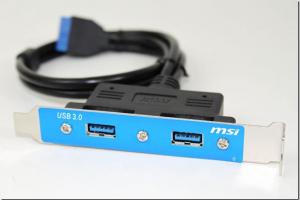
184-pin DDR memory module
DDR SDRAM(from English Double Data Rate Synchronous Dynamic Random Access Memory- synchronous dynamic memory with random access and double data transfer rate) - type random access memory, used in computers. When using DDR SDRAM, double the operating speed is achieved than in conventional SDRAM, due to reading commands and data not only along the edge, as in SDRAM, but also along the clock signal cutoff. Due to this, the data transfer speed is doubled without increasing the frequency of the memory bus clock signal. Thus, when DDR operates at 100 MHz, we will get an effective frequency of 200 MHz (when compared with the SDR SDRAM analogue). In the specification JEDEC There is a remark that it is incorrect to use the term “MHz” in DDR; it is correct to indicate the speed of “millions of transmissions per second through one data output.”
The memory bus width is 64 bits, that is, 8 bytes are simultaneously transferred along the bus in one clock cycle. As a result, we obtain the following formula for calculating the maximum transfer speed for a given memory type: memory bus clock speed x 2 (data transfer twice per clock cycle) x 8 (number of bytes transmitted per clock cycle). For example, to ensure data transfer twice per clock cycle, a special “2n Prefetch” architecture is used. The internal data bus is twice as wide as the external one. When transmitting data, the first half of the data bus is transmitted first on the rising edge of the clock signal, and then the second half of the data bus on the falling edge.
In addition to double data transfer, DDR SDRAM has several other fundamental differences from simple SDRAM. They are mainly technological. For example, a QDS signal has been added and is located on the PCB along with the data lines. It is used for synchronization during data transfer. If two memory modules are used, then the data from them arrives at the memory controller with a slight difference due to the different distance. A problem arises in choosing a clock signal for reading them. Using QDS successfully solves this.
JEDEC sets standards for DDR SDRAM speeds, divided into two parts: the first for memory chips, and the second for memory modules, which, in fact, house the memory chips.
Memory chips
Each DDR SDRAM module contains several identical DDR SDRAM chips. For modules without error correction ( ECC) their number is a multiple of 8, for modules with ECC - a multiple of 9.
Memory chip specification
DDR200: DDR SDRAM memory operating at 100 MHz
DDR266: DDR SDRAM memory operating at 133 MHz
DDR333: DDR SDRAM memory operating at 166 MHz
DDR400: DDR SDRAM memory operating at 200 MHz
DDR533: DDR SDRAM memory operating at 266 MHz
DDR666: DDR SDRAM memory operating at 333 MHz
DDR800: DDR SDRAM memory operating at 400 MHz
Unlike other types of DRAM that used asynchronous data exchange, the response to the control signal received by the device is not returned immediately, but only when the next clock signal is received. Clock signals make it possible to organize the operation of SDRAM in the form of a finite state machine that executes incoming commands. In this case, incoming commands can arrive in a continuous stream, without waiting for the previous instructions to complete execution (pipelining): immediately after the write command, the next command can arrive, without waiting for the data to be written. The receipt of a read command will cause the data to appear at the output after a certain number of clock cycles - this time is called latency. SDRAM latency ) and is one of the important characteristics of this type of device.
Update cycles are performed on the entire row at once, unlike previous types of DRAM that updated data against an internal counter using the CAS-before-RAS update method.
Usage history
Mass production of SDRAM began in 1993. Initially, this type of memory was offered as an alternative to expensive video memory (VRAM), but SDRAM soon gained popularity and began to be used as RAM, gradually replacing other types of dynamic memory. Subsequent DDR technologies made SDRAM even more efficient. The development of DDR SDRAM was followed by the DDR2 SDRAM standard, and then the DDR3 SDRAM standard.
SDR SDRAM
The first SDRAM standard, with the advent of subsequent standards, became known as SDR (Single Data Rate - as opposed to Double Data Rate). One control command was received per clock cycle and one data word was transmitted. Typical clock speeds were 66, 100 and 133 MHz. SDRAM chips were available with data buses of various widths (typically 4, 8, or 16 bits), but typically these chips were part of a 168-pin DIMM module that could read or write 64 bits (without parity) or 72 bits (with parity check) in one clock cycle.
Using the data bus in SDRAM turned out to be complicated by a delay of 2 or 3 clock cycles between the read signal and the appearance of data on the data bus, while there should be no delay during write. It required the development of a rather complex controller that would not allow the data bus to be used for writing and reading at the same time.
Control signals
Commands that control the SDR SDRAM memory module are supplied to the module contacts via 7 signal lines. One of them sends a clock signal, the leading (rising) edges of which set the time points at which control commands are read from the remaining 6 command lines. The names (in parentheses are the names) of the six command lines and descriptions of the commands are given below:
- CKE(clock enable) - when the signal level is low, the supply of a clock signal to the chip is blocked. Commands are not processed, the state of other command lines is ignored.
- /CS(chip select) - when the signal level is high, all other control lines except CKE are ignored. Acts as a NOP (no operator) command.
- DQM(data mask) - a high level on this line prohibits reading/writing data. When a write command is issued at the same time, the data is not written to DRAM. The presence of this signal in the two clock cycles preceding the read cycle results in the data not being read from memory.
- /RAS(row address strobe) - despite the name, this is not a strobe, but just one command bit. Together with /CAS and /WE, it encodes one of 8 commands.
- /CAS(column address strobe) - despite the name, this is not a strobe, but just one command bit. Together with /RAS and /WE, it encodes one of 8 commands.
- /WE(write enable) - Together with /RAS and /CAS, encodes one of 8 commands.
SDRAM devices are internally divided into 2 or 4 independent memory banks. The address inputs of the first and second memory bank (BA0 and BA1) determine which bank the current command is intended for.
The following commands are accepted:
| /CS | /RAS | /CAS | /WE | B.A. n | A10 | A n | Team |
|---|---|---|---|---|---|---|---|
| IN | x | x | x | x | x | x | command delay (no operation) |
| N | IN | IN | IN | x | x | x | no operation |
| N | IN | IN | N | x | x | x | stop the current batch read or write operation. |
| N | IN | N | IN | Bank number | N | Column no. | read a data packet from the currently active row. |
| N | IN | N | IN | Bank number | IN | Column no. | |
| N | IN | N | N | Bank number | N | Column no. | write a data packet to the currently active row. |
| N | IN | N | N | Bank number | IN | Column no. | like the previous command, and upon completion of the command, regenerate and close this row. |
| N | N | IN | IN | Bank number | Row No. | open the row for write and read operations. | |
| N | N | IN | N | Bank number | N | x | deactivate the current row of the selected bank. |
| N | N | IN | N | x | IN | x | deactivate the current row of all banks. |
| N | N | N | IN | x | x | x | regenerate one row of each bank using the internal counter. All banks must be deactivated. |
| N | N | N | N | 0 0 | MODE | from lines A0-A9 load configuration parameters into the chip. The most important are CAS latency (2 or 3 clock cycles) and packet length (1, 2, 4 or 8 clock cycles) |
|
Examples
Links
| Types of Dynamic Random Access Memory (DRAM) | |
|---|---|
| Asynchronous | FPM RAM · EDO RAM |
| Synchronous | SDRAM · DDR SDRAM · Mobile DDR (LPDDR) · DDR2 SDRAM · DDR3 SDRAM · DDR4 SDRAM |
| Graphic | VRAM · WRAM · MDRAM · SGRAM · GDDR · GDDR2 · GDDR3 · GDDR4 · GDDR5 |
| Rambus | RDRAM · XDR DRAM · XDR2 DRAM |
Wikimedia Foundation. 2010.
See what "SDRAM" is in other dictionaries:
SDRAM- Saltar a navegación, búsqueda Memoria SDRAM. Synchronous dynamic random access memory (SDRAM) es la dynamic random access memory (DRAM) que tiene una interfaz sincrónico. Tradicionalmente, la memoria dinámica de acceso aleatorio (DRAM) tiene una… … Wikipedia Español
SDRAM- refers to synchronous dynamic random access memory, a term that is used to describe dynamic random access memory that has a synchronous interface. Traditionally, dynamic random access memory (DRAM) has an asynchronous interface which means that... ... Wikipedia
SDRAM- Modul SDRAM Speichermodule auf einer Hauptplatine SDRAM ist die Abkürzung für „Synchronous Dynamic Random Access Memory“, eine Art des … Deutsch Wikipedia
SDRAM- , neuere, besonders schnell arbeitende Variante von DRAM Speicher Chips (DRAM) mit Zugriffzeiten von 7 12 ns. SDRAM Chips werden… … Universal-Lexikon
SDRAM- (Synchronous Dynamic Random Access Memory) Random Access Memory that can be adjusted and synchronized with the speed of the computer clock … English contemporary dictionary
SDRAM- Sigles d’une seule lettre Sigles de deux lettres Sigles de trois lettres Sigles de quatre lettres > Sigles de cinq lettres Sigles de six lettres Sigles de sept… … Wikipédia en Français